# Let's Start From Sand
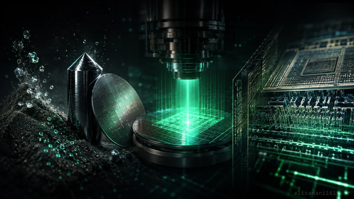
If we trace the path all the way back to the beginning, we arrive at something you might not expect: sand. The silicon used in the semiconductor industry is derived from materials like silica — the substance that makes up a large portion of sand and quartz.
But the distance between a grain of sand and the processor inside your computer is not just a simple industrial process. Along this path, chemistry, physics, optics, materials engineering, software, robotics, and machines of extraordinary precision all come together.
Key insight: What is built at the end can pack billions of transistors into a space of just a few centimeters. So let's look at the CPU from a place where it's rarely seen.
# What Exactly Is a CPU?
A CPU, or Central Processing Unit, is the component that executes program instructions. When you run a program, the processor is constantly receiving, interpreting, and executing instructions. In the simplest view:
1
Fetch — instruction is read from memory
2
Decode — instruction is interpreted
3
Execute — operation runs in the ALU
4
Store — result is written to register or memory
But the CPU doesn't do this with a few large, visible components. At the lowest level, everything comes down to transistors. A transistor can be thought of as a tiny electronic switch — a switch that can control the flow of current.
T
Transistor
Tiny electronic switch — controls current flow
G
Logic Gate
AND, OR, NOT, XOR — built from transistors
C
Digital Circuit
Complex circuits — adders, multiplexers
U
Processing Unit
ALU, registers, controllers
★
CPU Core
Complete processing core with Cache
# Before the CPU: How Did Computers Calculate?
Early computers didn't have anything like today's processors. One of the most famous examples was ENIAC, built in the 1940s, which used a massive number of vacuum tubes. What you see today in a tiny chip could once fill an entire room of electronic equipment.
Vacuum Tubes — 1940s
Large, fragile, power-hungry, short-lived
- A room full of equipment
- Thousands of vacuum tubes
- Extremely high power consumption
Transistor — 1947
Small, durable, efficient, cheap
- Much smaller footprint
- Low power consumption
- High reliability
In 1947, Walter Brattain, John Bardeen, and William Shockley at Bell Labs developed the transistor. But there was still a problem: if you wanted to connect thousands of transistors with wires, the circuit would quickly become unmanageable. The solution was the Integrated Circuit (IC).
# The First Microprocessor: Intel 4004
In 1969, the Japanese company Busicom asked Intel to design a set of integrated circuits for their 141-PF calculator. But Intel engineers pursued a different idea: instead of a large set of custom circuits, they moved some of the functionality to a programmable processor.
The result was the Intel 4004, introduced in November 1971:
2,300
Transistors
10μm
Process Node
740 kHz
Clock Speed
4-bit
Data Width
Today, 2,300 transistors seems like a tiny number. But in 1971, placing that many transistors on a single chip was a historic milestone. The 4004 proved that what previously required a massive collection of circuits could fit on a single small chip.
# From 2,300 Transistors to Billions
After the 4004, processors evolved at a rapid pace:
'71
Intel 4004
≈ 2,300 transistors — 10μm
'74
Intel 8080
≈ 4,500 transistors — 6μm
'78
Intel 8086
≈ 29,000 transistors — foundation of x86
'10
Intel Xeon
≈ 2,300,000,000 transistors
★
Modern CPUs
Billions of transistors — 3nm process
This growth didn't just mean faster CPUs. More transistors meant the ability to build:
Larger Cache
- L1, L2, L3
- Faster access
More Cores
- Multi-core
- Parallel processing
Integrated Graphics
- GPU on chip
- Vector processing
AI Accelerators
- NPU, TPU
- Machine learning
# Silicon, Crystals, and Wafers
The primary material for most semiconductor chips is silicon. Silicon isn't available in nature in the pure form needed for chip manufacturing. First, silicon must be extracted and purified to an extreme degree. Why is purity so important? Because we're building structures at the nanometer scale, and even a tiny amount of impurity can change the electrical properties of the material.
What is a Wafer? A wafer is a very thin disc of single-crystal silicon with a mirror-polished surface. It serves as the "canvas" for chip manufacturing — all transistors and circuits are built on this surface. Advanced wafers typically have a diameter of 300mm and can hold hundreds of chips.
Pure silicon is melted, and using methods like the Czochralski process, a large single-crystal ingot of silicon is grown. This cylinder is called a Silicon Ingot. The ingot is then sliced into very thin discs called Wafers.
1
Sand / Silica — raw material from nature
2
Pure Silicon — 99.9999999% purity
3
Silicon Ingot — single-crystal cylinder
4
Wafer — sliced and polished disc
300mm
Wafer Diameter
9N
Silicon Purity
~100
Chips Per Wafer
You can think of the wafer as a canvas. But the painting that will be done on it cannot be seen with the naked eye, and the paintbrush is not an ordinary brush — it's light.
# The Factory Where Even Dust Is the Enemy
Chip manufacturing takes place in an environment called a Cleanroom. In this environment, air, temperature, humidity, and contamination levels are strictly controlled. Wafers are moved automatically by robotic systems during many stages.
Why all this sensitivity? Because something that is nearly invisible to a human can be a massive obstacle at the scale of chip manufacturing. The chip production process involves hundreds of steps and can take months from design to production.
# A CPU Is Not Built All at Once
This is one of the most important points about chip manufacturing. No one picks up a wafer and prints billions of transistors on it in one go. A chip is built layer by layer:
1
Deposition — deposit material on surface
2
Lithography — pattern with light
3
Etching — remove unwanted material
4
Doping — modify electrical properties
5
Cleaning & Inspection — prepare and verify
↻
Repeat — this cycle runs hundreds of times
In reality, a CPU is not carved — it's shaped layer by layer.
# Lithography: When Light Draws Circuits
One of the key steps in chip manufacturing is Photolithography. The wafer surface is coated with a light-sensitive material called Photoresist. Then, a very precise pattern is created on it using light.
The smaller the features we want to create, the harder it becomes to control the light. For advanced chip generations, one of the most important technologies is EUV — Extreme Ultraviolet Lithography:
13.5nm
EUV Wavelength
~10
Precision Mirrors
50,000×
Laser Pulses / Second
In EUV machines, generating the light itself is an incredibly complex process. Tiny droplets of tin are hit by laser pulses, creating a plasma that emits EUV light. This light cannot be guided with glass lenses like ordinary light — instead, highly specialized mirror systems are used.
This is where CPU manufacturing transforms from a simple electronic process into a combination of plasma physics, lasers, optics, and mechanical engineering.
# Now It's Time to Build Transistors
In the simplest view, a transistor is a switch:
OFF
No current flows
0
ON
Current is controlled
1
By controlling the electrical properties of the semiconductor material, current can be controlled. One of the important processes here is Doping — a carefully controlled amount of specific atoms is introduced into the silicon structure to change its electrical properties.
2D
Planar MOSFET
Flat transistor — older generations
3D
FinFET
3D fin-shaped structure — better current control
★
Gate-All-Around (GAA)
Gate wraps around all sides — most advanced today
# Transistors Alone Are Not a CPU
Suppose we've built billions of transistors. Is the CPU ready? No. Transistors need to communicate with each other. This is where another part of the chip enters the story: Interconnects.
M3
Metal Layer 3 — Highways
Long-range connections — signals across distant blocks
M2
Metal Layer 2 — Arterial Roads
Medium connections — inter-neighborhood
M1
Metal Layer 1 — Streets
Short connections — direct link to transistors
T
Transistors — Buildings
Billions of electronic switches
Si
Silicon Substrate — Ground
Silicon base of the wafer
Transistors are the buildings of this city. Metal interconnects are the streets, and electrical signals travel through this network. If this network isn't designed correctly, even billions of powerful transistors can't make a good CPU.
# A CPU Is Designed Before It's Built
The factory doesn't know on its own where to place transistors. Before a single wafer enters the production line, the CPU must be designed:
1
Architecture — what the CPU should do
2
Instruction Set (ISA) — instruction set design
3
RTL Design — describe circuit behavior
4
Simulation & Verification — test and validate
5
Physical Design — convert to physical layout (EDA)
6
Mask Data → Manufacturing — build masks and produce
In other words, before a CPU is a piece of silicon, it is first a massive computational design.
# Yield, Dicing, and Packaging
On a large wafer, many Dies are placed. Then it must be determined which dies are functional. The percentage of usable dies relative to all dies produced is called Yield.
1
Wafer Test — test all dies on the wafer
2
Dicing — cut and separate dies
3
Packaging — place die in protective housing
4
Final Testing — test performance, temp, frequency
The package is not just a protective frame — it must also handle electrical connections, signal transfer, heat dissipation, and mechanical protection. Today, the Chiplet concept allows different parts of the processor to be built on separate dies and connected within a single package.
Monolithic Die
Everything on one piece of silicon
- Unified design
- Lower yield for large dies
Chiplet
Multiple small dies in one package
- Higher yield
- More flexibility
# Moore's Law and New Challenges
In 1965, Gordon Moore made an observation that later became known as Moore's Law: the number of transistors that can be placed on a chip would increase rapidly over time. This wasn't a precise physical law — it was more of an observation and prediction about industry trends.
But as structures got smaller, new problems emerged:
Heat
- Harder thermal management
Current Leakage
- Atoms are too small
Equipment Cost
- EUV machines are extremely expensive
Physical Limits
- Approaching atomic scale
Why does a CPU get hot? Every time transistors switch states, energy is consumed, and some of it is converted to heat. That's why a CPU needs a heatsink and cooling system.
# A CPU Isn't Built From Sand — It's Built From Information
The strangest part of all is that a CPU isn't built from sand — it's built from information. The raw material is silicon. But what turns it into a CPU is the design pattern, the manufacturing instructions, the masks, the transistor positions, and billions of engineering decisions.
We haven't just made matter smaller. We've written information into matter. It started with sand; it arrived at computation.
takeaway.txt
Sometimes, building a computational machine requires nothing more
than a piece of silicon — if you know how to shape it
at the scale of billions of transistors.
than a piece of silicon — if you know how to shape it
at the scale of billions of transistors.